
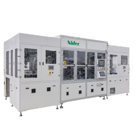
Semiconductor package multi-surface full panel substrate inspection device
Support for a total of 48K points in both vertical and horizontal directions! A high-speed inspection solution for multi-panel arrangements of large full-panel PCBs (500×620mm).
We would like to introduce our semiconductor package multi-site full panel substrate inspection equipment, the 'GATS-8370'. It is optimal for next-generation semiconductor packages with larger unit sizes and more pins. This high-precision electrical inspection device supports bulk and high-speed inspection of full panel substrates. It achieves efficient step-and-repeat inspection with a single shuttle, balancing quality improvement and reduced takt time. 【Features】 ■ Comprehensive inspection with a large capacity of 48K points (49,152p) ■ Bulk inspection of large unit products (up to 300mm) ■ Compatible with large full panel sizes (500mm × 620mm) *For more details, please download the PDF or feel free to contact us.
- Company:ニデックアドバンステクノロジー 本社、東京営業所、名古屋営業所
- Price:Other
